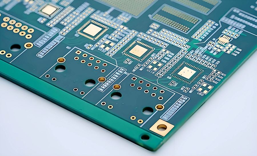
High-Density Interconnect (HDI) PCB: The Backbone of Modern Miniaturized Electronics
High-Density Interconnect (HDI) PCB has transformed modern electronics by enabling more functionality in smaller spaces while delivering higher performance and superior reliability. As devices continue to shrink and processing speeds increase, traditional circuit boards can no longer meet the requirements of today’s high-speed digital systems. HDI technology offers an innovative solution through ultra-fine traces, microvias, and multilayer stacking. These advanced design features allow manufacturers to place more components within limited board areas, making HDI essential for smartphones, medical devices, automotive electronics, industrial automation, military systems, and next-generation communication equipment.
Why High-Density Interconnect (HDI) PCB Technology Matters
High-Density Interconnect (HDI) PCB technology matters because it supports the evolution of compact, high-performance devices. With conventional PCBs, the space needed for routing limits how complex circuits can become. HDI bypasses these limitations using high-density routing and advanced via structures such as microvias, blind vias, and buried vias. These microscopic interconnections reduce the distance signals must travel, improving speed and reducing loss. The result is superior electrical performance, better noise control, and enhanced signal integrity even at high frequencies, which is crucial for 5G devices, computing systems, sensors, and artificial intelligence hardware.
How HDI PCB Enhances Electronic Performance
The electrical advantages of High-Density Interconnect (HDI) PCB technology are substantial. Shorter signal paths decrease impedance, and microvias ensure precise communication between layers with minimal distortion. This leads to faster signal transmission, making HDI ideal for applications where every nanosecond matters. Data centers, networking systems, and advanced processors rely heavily on HDI boards because they maintain stability under demanding workloads. The minimized parasitic effects and controlled impedance offered by HDI layouts ensure seamless high-speed performance for critical systems.
Thermal Performance Advantages
Modern electronics generate heat due to increased component density and higher processing speeds. High-Density Interconnect (HDI) PCB structures manage thermal distribution more efficiently than traditional boards. Through optimized copper balancing, improved pad design, and controlled layer stacking, HDI helps components maintain stable operating temperatures. This improves longevity and prevents overheating issues in compact devices. Industries such as automotive electronics, especially those utilizing ADAS modules and EV control systems, benefit greatly from HDI’s excellent thermal behavior.
Mechanical Strength and Reliability
Beyond electrical and thermal advantages, High-Density Interconnect (HDI) PCB improves overall board durability. Microvias are structurally stronger than traditional vias due to their small diameter and shallow depth. This makes HDI resistant to thermal cycling, vibrations, and mechanical stress. With reliability being critical for aerospace, medical, and industrial electronics, HDI PCB technology ensures consistent performance even in harsh environments.
HDI PCB in Modern Miniaturization
The trend toward smaller and more powerful products demands advanced circuit designs that traditional PCBs cannot achieve. High-Density Interconnect (HDI) PCB technology enables ultra-compact layouts by placing microvias directly under components, integrating multiple layers, and using finer line spacing. This makes it possible to build slim smartphones, compact medical implants, miniaturized IoT sensors, lightweight wearables, and high-capacity memory modules. As designs shrink in size, HDI facilitates efficient routing and component placement without sacrificing performance.
Complex Component Compatibility
Many high-performance components such as BGAs, CSPs, and QFNs have densely packed pads that require precise routing. High-Density Interconnect (HDI) PCB technology supports these components by enabling breakout routing using high-density microvias. This compatibility with advanced packaging technologies allows engineers to create powerful systems within limited space, enhancing both speed and efficiency.
Applications of High-Density Interconnect (HDI) PCB
The versatility of High-Density Interconnect (HDI) PCB makes it a core technology across multiple industries. In consumer electronics, HDI is used in smartphones, tablets, laptops, and gaming devices to deliver high power in sleek designs. Medical fields depend on HDI for diagnostic equipment, imaging systems, portable monitors, and implantable devices. Automotive applications include navigation systems, ADAS modules, dashboard controls, and EV battery management systems. Defense and aerospace sectors use HDI for communication tools, radar systems, and avionics. Industrial automation, robotics, telecommunication networks, and artificial intelligence hardware also rely on HDI due to its superior performance and reliability.
Types of HDI PCB Structures
There are several HDI structures, and each offers different advantages depending on the application. The simplest form uses one sequential lamination with microvias connecting the outer layers to inner layers. More advanced types use multiple sequential laminations with stacked microvias for increased density. Some HDI boards incorporate a combination of blind, buried, and stacked vias to achieve complex routing paths. These structures allow engineers to customize designs according to performance, density, and thermal requirements. As devices become more powerful, the need for advanced HDI configurations continues to rise.
Design Considerations for High-Density Interconnect (HDI) PCB
HDI design requires expertise and precision. Engineers must optimize trace widths, pad sizes, layer stack-ups, and impedance control. Microvia reliability is influenced by drilling accuracy, copper plating thickness, and lamination cycles. Material selection also plays a key role, especially in high-frequency applications where low-loss laminates such as Rogers or hybrid materials are preferred. Signal integrity simulations, thermal analysis, and manufacturing tolerance adjustments are essential during HDI design to ensure the final product performs as intended.
Future Trends in High-Density Interconnect (HDI) PCB Technology
The future of High-Density Interconnect (HDI) PCB technology is closely tied to advancements in artificial intelligence, EVs, medical innovations, and high-speed communication networks. As 6G, robotics, and automated systems grow, the demand for HDI boards capable of supporting ultra-high-speed processing will continue to increase. Improved materials, laser drilling technology, and stacked via capabilities will shape the next generation of HDI designs. The shift toward miniaturization and increased functionality will make HDI more critical than ever.
Conclusion
High-Density Interconnect (HDI) PCB technology plays an essential role in building compact, high-performance, and energy-efficient electronic systems. Its advantages in signal integrity, thermal management, durability, and miniaturization make it the preferred solution for modern industries seeking speed, reliability, and advanced functionality. For companies aiming to develop next-generation products, partnering with an experienced HDI PCB Manufacturer ensures precision, consistency, and exceptional quality from prototype to mass production.


